VLSI (Very-Large Scale-Integration) design involves creating complex integrated circuits (ICs) by integrating millions or even billions of transistors onto a single chip. Different design styles in VLSI are employed depending on the application requirements, cost considerations, power consumption, performance needs, and flexibility. These styles can be broadly classified into five categories:
a) Full-Custom Design
b) Semi-Custom Design
c) Programmable Logic Devices (PLD) Design
d) System-on-Chip (SoC) Design
e) Off-the-shelf Design
Fig 5.1 shows the classification of VLSI Design styles followed by elaborate explanation of each design methodologies.
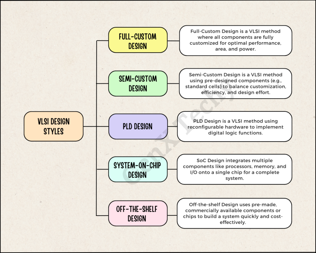
Fig. 5.1: Classification of VLSI Design Styles
a) Full-Custom Design
(i) In full-custom design, the entire chip is precisely crafted from the ground up, without relying on pre-designed standard cell libraries. Every component, including transistors, logic gates, and interconnects, is manually designed and optimized. This method allows unparalleled control over the chip’s architecture, enabling designers to achieve the highest levels of efficiency in terms of area, power consumption, and performance (delay, thermal affects, etc).
(ii) This meticulous optimization makes full-custom design the most advanced and precise design style, offering superior results compared to other approaches. However, this comes at the cost of significantly longer development times and increased complexity. Each step, from schematic creation to layout design, requires extensive effort, expertise, and verification, leading to a prolonged design cycle.
(iii) Despite these challenges, full-custom design is the preferred choice for products that demand exceptional performance, such as high-speed processors, advanced GPUs, and custom memory units. It is particularly advantageous for high-volume manufacturing, where the high initial design costs can be distributed across large-scale production, making it economically viable while delivering the best possible performance.
b) Semi-Custom Design
(i) In semi-custom design, a significant portion of the chip is developed using pre-designed and pre-verified components, such as standard cell libraries, memory blocks, and intellectual property (IP) cores. Designers focus on the placement and interconnection of these components to achieve the desired functionality. This approach balances customization and efficiency, offering a middle ground between full-custom and off-the-shelf design styles.
(ii) Semi-custom design significantly reduces development time and complexity compared to full-custom design. By leveraging standard cells for commonly used logic functions, designers avoid the need to create circuits from scratch, expediting the design process while ensuring reliability. However, this style offers less flexibility and optimization, as the standard cells are not tailored to the specific application.
(iii) While semi-custom designs may not achieve the same level of performance, power efficiency, or area optimization as full-custom designs, they are cost-effective and faster to implement. This makes them ideal for applications that demand moderate performance and quick time-to-market, such as general-purpose ASICs, consumer electronics, and communication devices.
(iv) The semi-custom design style is widely used in VLSI because it combines the reliability of pre-verified components with the flexibility to customize interconnects and overall architecture. This approach provides an efficient pathway for developing complex chips with a good balance of performance, cost, and development time.
c) Programmable Logic Devices (PLD) Design
(i) In Programmable Logic Device (PLD) design, the chip is pre-fabricated with configurable logic blocks, interconnects, and memory elements, which can be programmed to implement desired functionality after manufacturing. This design style provides unparalleled flexibility, as it allows designers to reprogram the chip multiple times to adapt to changing requirements or fix design flaws.
(ii) PLD design eliminates the need for lengthy fabrication cycles, making it ideal for rapid prototyping, low-volume production, and applications where adaptability is critical.
(iii) PLDs consist of an array of logic gates and interconnects that can be programmed to perform specific functions. The programmability allows designers to implement complex digital circuits without designing custom ICs. PLDs are broadly classified into three categories:
Simple Programmable Logic Devices (SPLDs):
- These devices have a limited number of logic gates and are suitable for small-scale designs.
- SPLDs consists of:
PROM (Programmable Read-Only Memory): A memory device that can be programmed once to implement combinational logic.
PAL (Programmable Array Logic): Consists of a programmable AND array and a fixed OR array.
PLA (Programmable Logic Array): Features both programmable AND & OR arrays, offering greater flexibility than PAL.
Complex Programmable Logic Devices (CPLDs):
- CPLDs consist of multiple SPLD-like blocks connected via a programmable interconnect.
- They offer higher logic density and are used for medium-complexity designs.
Field-Programmable Gate Arrays (FPGAs):
- FPGAs are the most advanced PLDs, featuring a large number of configurable logic blocks (CLBs), programmable interconnects, and I/O blocks.
- They are capable of implementing highly complex digital systems, including processors, DSPs, and communication protocols.
d) System-on-Chip (SoC) Design
(i) System-on-Chip (SoC) Design is a multidisciplinary process that integrates multiple components of a computer system, such as processing units, memory, interfaces, and custom logic, onto a single silicon chip. This design approach enables compact, power-efficient, and high-performance solutions, making it ideal for modern applications like smartphones, IoT devices, automotive systems, and industrial automation. By combining diverse functionalities within a single chip, SoCs reduce the overall size and cost of electronic systems while improving performance through optimized data communication.
(ii) The design process begins with defining system requirements and architecture, including selecting the right processor cores (e.g., CPUs, GPUs, or AI accelerators) and other hardware blocks. These components are interconnected using advanced interconnect technologies such as buses or networks-on-chip (NoC). Memory integration, including SRAM, DRAM, or embedded Flash, is crucial for ensuring data availability and high-speed processing. Peripheral interfaces like USB, HDMI, or PCIe are included to support connectivity, while power management circuits ensure energy efficiency.
(iii) SoC design is extensively used in application-specific products, such as those for image processing, machine learning, or real-time systems. For example, AI-enabled SoCs in autonomous vehicles integrate vision processors and neural network accelerators to handle real-time decision-making. Similarly, in smartphones, SoCs combine powerful processors, image signal processors (ISPs), and wireless communication modules to deliver seamless user experiences.
(iv) With the increasing demand for complex, high-performance systems, the SoC design process incorporates advanced techniques such as hardware-software co-design, IP reuse, and Design for Testability (DFT). These methodologies ensure not only the efficient performance of the chip but also ease of debugging, scalability, and shorter time-to-market for innovative solutions.
e) Off-the-shelf Design
(i) Off-the-Shelf Design Styles play a crucial role in accelerating the development of modern electronic systems by leveraging pre-designed, pre-verified components, also known as Intellectual Property (IP) blocks. These design styles are extensively used in applications requiring rapid prototyping, cost-effectiveness, and flexibility. Examples include embedded systems, consumer electronics, automotive systems, and industrial automation.
(ii) In the consumer electronics industry, off-the-shelf components like Wi-Fi modules, Bluetooth interfaces, and display drivers allow designers to quickly assemble products like smart TVs, wearables, and smartphones. For automotive applications, reusable IP blocks such as ADAS (Advanced Driver Assistance Systems) modules, radar systems, and real-time processors streamline the design of safety-critical and infotainment systems.
(iii) In industrial automation, pre-built components like motor controllers, sensor interfaces, and communication protocols (e.g., Modbus, Ethernet/IP) enable seamless integration of robotic systems and IoT-enabled devices. Similarly, in medical devices, off-the-shelf design is used to incorporate standardized components like imaging processors, bio-signal acquisition modules, and wireless connectivity, reducing time-to-market for critical healthcare solutions.
(iv) By focusing on system integration and functionality rather than low-level design, off-the-shelf design styles empower engineers to quickly adapt to market needs, ensuring robust and scalable solutions for diverse applications.
(v) Despite its advantages, off-the-shelf design styles may have limitations, such as compatibility issues or reduced optimization for specific use cases. Designers must carefully evaluate the trade-offs between customization and the convenience of pre-built components. Nonetheless, as technology evolves, off-the-shelf design continues to play a pivotal role in accelerating innovation and addressing the complexity of modern electronic systems.