VLSI (Very-Large-Scale-Integration) design flow is the process of creating integrated circuits (ICs) by combining thousands or millions of transistors into a single chip. It involves a sequence of well-defined steps that ensure the functionality, performance, and manufacturability of the chip. Figure 4.1 shows the flow diagram of VLSI design and a discussion on each design step is also explained elaborately.
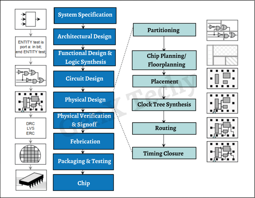
Figure 4.1 VLSI Circuit Design Flow
1. System Specification:
System Specification is the foundational step in the VLSI design flow, defining the system’s functionality, performance goals, and constraints.
- It establishes a clear framework for the design process, outlining what the system must achieve in terms of input/output behavior, data processing, and communication protocols.
- Key performance metrics such as speed, power consumption, and chip area are specified to align with the application’s requirements.
- The technology node (e.g., 7nm or 28nm) and fabrication details ensure compatibility with manufacturing processes.
- Interface specifications define interactions with external components and protocols, while constraints like cost, scalability, and environmental conditions shape practical development.
- The system specification also includes a high-level block diagram and a verification plan to validate the design. By addressing potential challenges early, it reduces risks, minimizes revisions, and optimizes resource allocation, serving as a critical reference throughout the VLSI design process for efficient and successful implementation.
2. Architectural Design:
Architectural Design is a critical step in the VLSI design flow, translating the system specifications into a high-level structural framework. Significant aspects include:
- Functional Partitioning: Breaks down the system into smaller functional blocks (e.g., processor, memory, I/O controllers).
- Data Path Design: Defines how data flows between blocks and the components involved (e.g., buses, registers).
- Control Path Design: Specifies the control logic for coordinating data flow and operations within the system.
- Performance Analysis: Evaluates latency, throughput, and power consumption to meet system specifications.
- Optimization: Balances trade-offs between performance, area, and power consumption.
- Technology Consideration: Selects suitable technology for implementation, factoring in speed and power efficiency.
- Interface Definition: Designs interfaces for communication between blocks and with external components.
- Verification Plan: Outlines initial tests to ensure the architecture meets the functional and performance goals.
The architectural design provides a detailed blueprint, guiding the transition to RTL (Register Transfer Level) design.
3. Functional and Logic Design:
- After the architecture is established, the functionality and interconnections of individual modules (e.g., a processor core) must be specified. In this stage, only the high-level behaviour is defined, focusing on the inputs, outputs, and timing characteristics of each module.
- The logic design phase is carried out at the Register-Transfer Level (RTL) using hardware description languages (HDLs) such as Verilog or VHDL. This involves writing programs that describe the chip’s functionality and timing behaviour. These HDL modules must undergo extensive simulation and verification to ensure correctness.
- Logic synthesis tools automate the transformation of HDL descriptions into low-level circuit components. These tools take the HDL code and a technology library as input and generate a netlist, which represents the connectivity of signal nets and circuit elements, including standard cells and transistors. This process bridges high-level design with physical implementation.
4. Circuit Design:
- Logic Synthesis and Gate-Level Netlist Generation. For most digital logic on a chip, logic synthesis tools are used to automatically translate Boolean expressions into a gate-level netlist. The netlist represents the circuit’s structure at the level of standard cells or higher, ensuring the design is ready for physical implementation.
- Transistor-Level Circuit Design. Certain critical components must be meticulously designed at the transistor level, a process known as circuit design. This approach is necessary for elements that demand precise control over electrical characteristics.
- Verification of Circuit Design. The correctness of these transistor-level designs is verified using circuit simulation tools like SPICE. SPICE ensures accurate modeling of electrical behavior under various conditions, guaranteeing design reliability.
5. Physical Design:
- During physical design, all components of the design are instantiated with their precise geometric representations. This means that macros, cells, gates, transistors, and other elements, each with fixed shapes and sizes corresponding to fabrication layers, are assigned specific spatial locations (placement) and connected through appropriate routing using metal layers. The outcome of this phase is a detailed set of manufacturing specifications, which must be thoroughly verified for correctness.
- Design Rules and Fabrication Constraints: Design Rule Checking (DRC) ensures that the layout adheres to all the technology-specific constraints imposed by the fabrication process. This involves verifying the minimum spacing between components, layer thickness, and other physical design rules. Additionally, DRC checks the layer density to ensure compatibility with Chemical-Mechanical Polishing (CMP), a critical process that smooths and flattens layers during manufacturing. DRC is essential for ensuring that the design can be fabricated without defects that would compromise performance or manufacturability.
Impact of Physical Design on Key Metrics:
- Performance: Longer routing paths increase signal delay, impairing circuit speed.
- Area: If connected modules are placed too far apart, the chip area increases, leading to slower performance.
- Reliability: Excessive use of vias can drastically reduce the circuit’s reliability by increasing the risk of failure.
- Power: Smaller transistors offer faster switching speeds but come at the cost of higher leakage currents and variability; conversely, larger transistors and longer wires lead to greater dynamic power dissipation.
- Yield: Routing wires too close together can cause electrical shorts during manufacturing, while placing gates too far apart increases the chances of opens and reduces overall yield.
Due to its high complexity, physical design is split into several key steps (as shown in Fig. 4.1)
- Partitioning: Partitioning is the process of dividing a large, complex circuit into smaller, more manageable sub-circuits or modules. This enables each segment to be designed, analysed, and optimized independently, improving both efficiency and focus in the design process. Partitioning ensures that each smaller section of the circuit adheres to specific design constraints, and it helps reduce overall design complexity by isolating problems and streamlining the design flow.
- Chip Planning/Floor-Planning: Chip planning or floor-planning is the strategic arrangement of the various sub-circuits, modules, and IP (Intellectual Property) blocks within the physical layout of the chip. This step defines the shape, orientation, and relative positioning of components on the chip, as well as the locations of external ports. Effective floor-planning optimizes the chip’s area efficiency, minimizes interconnect delays, and enhances overall performance by ensuring that the modules are placed in a way that facilitates efficient routing and power distribution.
- Placement: Placement is the stage where the precise spatial locations of individual cells within each block of the circuit are determined. This step ensures that all cells are positioned optimally to meet physical constraints, such as wire length, routing congestion, and performance goals. Proper placement minimizes delay, improves power efficiency, and contributes to a more compact and functional chip design by ensuring that cells are arranged in a way that minimizes interconnect paths.
- Clock Tree/Network Synthesis: Clock tree/network synthesis is the process of designing the clock distribution network within a chip to ensure that the clock signal reaches all parts of the circuit with the required precision. This includes the buffering, gating (for power management), and routing of the clock signal, carefully managing clock skew and signal delay to meet stringent timing requirements. A well-designed clock tree ensures synchronized operation across the chip, improving performance while minimizing power consumption and timing violations.
- Global Routing: Global routing involves the allocation of routing resources for interconnecting different modules and components on the chip. This includes the assignment of routing tracks in channels and switchboxes to ensure that signals can be routed across the chip without excessive congestion or delay. Global routing provides a high-level plan for how signals will flow through the chip, and it forms the basis for the subsequent detailed routing process, which assigns specific metal layers and tracks for each signal.
- Detailed Routing: Detailed routingis the phase where the global routing plan is refined by assigning specific metal layers and routing tracks to each connection. This step ensures that the design is manufacturable and that all routing constraints are met, including signal integrity, resistance, capacitance, and physical limitations of the manufacturing process. Detailed routing optimizes the final layout by minimizing routing congestion, reducing power consumption, and ensuring that the chip functions reliably.
- Timing Closure: Timing closure is the process of fine-tuning the design through specialized placement and routing techniques to ensure that all timing requirements are met. This includes optimizing the delay paths, adjusting the placement of cells to minimize critical path delays, and refining the routing to achieve the necessary performance levels. Timing closure ensures that the circuit operates at the desired speed without violating setup or hold time constraints, making it a critical phase for achieving optimal performance and reliability in the final design.
6. Physical Verification:
Once the physical design is complete, the layout must undergo thorough verification to ensure it meets the required electrical and logical functionality. Some issues found during verification may be acceptable if they have little effect on the chip’s yield or performance. However, if the problems are significant, the layout must be modified. These changes should be minimal and carefully managed to avoid creating new issues. At this stage, experienced engineers typically make these adjustments manually, ensuring that the final design remains accurate and reliable.
- Design Rule Checking (DRC): Design Rule Checking (DRC) ensures that the layout adheres to all the technology-specific constraints imposed by the fabrication process. This involves verifying the minimum spacing between components, layer thickness, and other physical design rules. Additionally, DRC checks the layer density to ensure compatibility with Chemical-Mechanical Polishing (CMP), a critical process that smooths and flattens layers during manufacturing. DRC is essential for ensuring that the design can be fabricated without defects that would compromise performance or manufacturability.
- Layout vs. Schematic (LVS) Checking:Layout vs. Schematic (LVS) checking is a verification process that compares the physical layout of the design with the original schematic to ensure functional consistency. From the layout, a netlist is generated and compared with the netlist created during logic synthesis or circuit design. This check confirms that the physical design accurately reflects the intended circuit functionality and that no discrepancies exist between the two representations.
- Parasitic Extraction: Parasitic extraction is the process of determining the electrical parameters of the layout elements, such as resistance, capacitance, and inductance, based on their geometric representations. These parasitics are crucial for accurate circuit behaviour analysis, as they impact the speed and signal integrity of the design. Once extracted, parasitic elements are incorporated into the netlist and used for further analysis to verify the electrical characteristics and overall performance of the circuit.
- Antenna Rule Checking: Antenna Rule Checking addresses a potential issue known as the antenna effect, which occurs during the plasma-etch process in chip fabrication. This effect can accumulate excess charge on metal wires that are not connected to PN-junction nodes, potentially causing damage to transistor gates. Antenna rule checks ensure that metal traces are appropriately connected, preventing charge build-up and safeguarding the integrity of the gate structures during manufacturing.
- Electrical Rule Checking (ERC): Electrical Rule Checking (ERC) verifies that the circuit’s power and ground connections are correctly established and that electrical conditions such as signal transition times (slew rate), capacitive loads, and fanouts are within acceptable limits. ERC ensures the electrical integrity of the design by identifying issues like excessive current, incorrect signal timing, or inadequate power delivery, which could affect circuit performance, reliability, and functionality.
7. Fabrication:
The final DRC, LVS, and ERC-clean layout, typically in GDSII Stream format, is sent to the silicon foundry for manufacturing. This handoff, known as tapeout, marks the transition from design to production, though it no longer involves magnetic tape. The data transfer is often called streaming out, referring to the GDSII format. At the fab, the design is transferred onto layers of silicon through photolithography, using photomasks to expose specific patterns. Multiple masks are required, and any design changes necessitate modifying these masks. ICs are fabricated on silicon wafers, usually between 200 mm (8 inches) and 300 mm (12 inches). Afterward, the ICs are tested and categorized as functional or defective based on performance tests. Finally, the wafers are diced into individual ICs through sawing.
8. Packaging and Testing:
- After dicing, the functional chips are carefully packaged to protect and connect them for use in electronic devices. The packaging is determined early in the design process to meet specific application needs, cost constraints, and form factor requirements. Common types of packaging include dual in-line packages (DIPs), pin grid arrays (PGAs), and ball grid arrays (BGAs), each offering different ways to connect the chip to the external world.
- Once the die (the chip) is placed inside the package cavity, its pins need to be connected to the corresponding pins on the package. This is done using techniques like wire bonding, where tiny wires connect the die’s pads to the package’s pins, or flip-chip bonding, which uses solder bumps to make the connection. After the die is securely connected, the package is sealed to protect the chip from environmental damage, ensuring it remains functional and durable for its intended use. This packaging process plays a critical role in the overall performance and reliability of the chip in real-world applications.
- Chip testing is the process of verifying a chip’s functionality and performance after it has been manufactured. This ensures the chip meets the required specifications and works as intended. The testing process involves checking for defects, such as electrical shorts, incorrect signals, or power issues. Tests can include functional testing to check the chip’s logic, parametric testing to measure power, speed, and other characteristics, and stress testing to see how the chip performs under extreme conditions. Chips that pass testing are marked as functional, while defective ones are discarded or reworked.
Nice explanation
Thank you so much.
Team genxtechy.com