Bus Cycle
A bus cycle is the time taken by the microprocessor to complete one operation, like reading or writing data. Each operation happens over a few machine cycles (timing periods), controlled by the clock signals (T-states).
- When the 8085 wants to read data from memory, it performs a Memory Read Cycle.
- When it wants to store data into memory, it performs a Memory Write Cycle.
Important Buses Used
The 8085 communicates with memory using three main buses:
| Bus | Purpose | Lines |
|---|---|---|
| Address Bus | Carries the memory address from which data is to be read or to which data is to be written. | 16 bits (A15–A0) |
| Data Bus | Carries the actual data to or from the memory. | 8 bits (D7–D0) |
| Control Bus | Carries control signals that tell whether it’s a read or write operation. | Includes signals like RD’, WR’, IO/M’, etc. |
Control Signals Used
Different control signals used by 8085 during the memory read and memory write cycles are listed below:
| Signal | Type | Meaning (Active Low) |
|---|---|---|
| IO/M’ | Control | 0 → Memory operation, 1 → I/O operation |
| RD’ | Control | 0 → Read operation |
| WR’ | Control | 0 → Write operation |
| ALE (Address Latch Enable) | Control | Used to separate lower byte of address (A7–A0) from data bus (since AD0–AD7 are multiplexed) |
Memory Read Cycle of 8085 Microprocessor
The memory read cycle is the process by which the 8085 microprocessor reads or fetches data from a specific memory location. Whenever the microprocessor needs to read a byte of data or an instruction stored in memory, it performs this cycle.
- To begin the operation, the microprocessor places the 16-bit address of the required memory location on the address bus.
- The higher-order address (A15–A8) appears on the higher address lines, while the lower-order address (A7–A0) is multiplexed with the data bus lines (AD7–AD0).
- To separate the lower address from data, the microprocessor activates the ALE (Address Latch Enable) signal, which allows an external latch to store the lower address permanently for that cycle.
- Once the address is set, the control signal IO/M’ is made low to indicate that this is a memory-related operation. Then, during the next clock period, the RD’ (Read) control signal is made active low. This signal tells the memory device that the processor wants to read data from the specified address.
- The selected memory location then places its data byte onto the data bus. The 8085 reads this data and transfers it internally to one of its registers or uses it as an operand for further execution.
- After the data is successfully read, the RD’ signal returns to its inactive (high) state, and the data bus is released for the next operation.
- The complete process of addressing, enabling read, transferring data, and deactivating signals takes place within a few clock periods (T-states) and is known as the Memory Read Cycle.
Timing Cycle Details
To complete memory read operation 8085 microprocessor required few T-states (clock periods) those are listed below in table:
| T-State | Operation during each T-State |
|---|---|
| T1 | The microprocessor sends the address of the operand on the address bus and ALE goes high to latch the lower address. |
| T2 | RD’ goes low, instructing memory to place the operand on the data bus. |
| T3 | Memory places the operand on the data bus, the 8085 reads it, and RD’ goes high to release the bus. |
Control Signal Status
Status of 8085 microprocessor control signals during the memory read cycle are listed below:
| Signal | Meaning / Function |
|---|---|
| IO/M’ | 0 → Memory operation |
| RD’ | 0 (active low during operand fetch / memory read) |
| WR’ | 1 (no write) |
| ALE | High in T1 to latch address |
| Address Bus | Carries memory address of operand |
| Data Bus | Receives operand (data byte) |
Timing Diagram of Memory Read Cycle of 8085 Microprocessor
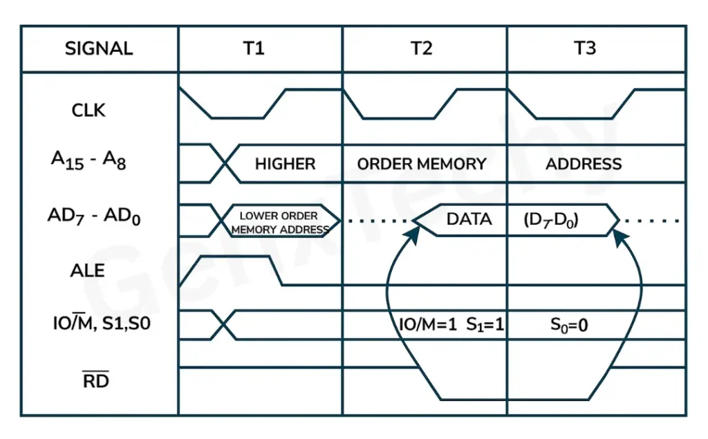
Figure 17.1: Timing Diagram of Memory Read Cycle of 8085 Microprocessor
Memory Write Cycle of 8085 Microprocessor
The memory write cycle is the process by which the 8085 microprocessor writes or stores a byte of data into a specific memory location. This cycle occurs when the microprocessor executes an instruction that requires sending data from one of its internal registers to the memory.
- To start the write operation, the 8085 first places the 16-bit address of the target memory location on the address bus.
- Just as in the read cycle, the lower-order address lines (AD7–AD0) are multiplexed with the data bus, so the ALE signal goes high during the first clock period to latch the lower address using an external latch. At the same time, the control signal IO/M’ is kept low, indicating a memory operation.
- After the address is established, the processor places the data to be written onto the data bus. Next, it makes the WR’ (Write) control signal active low. This tells the memory device that valid data is available on the data bus and should be stored at the specified address.
- The memory then accepts the data and writes it into that location. The data remains stable on the data bus for the entire duration that WR’ stays low.
- Once the write operation is completed, the microprocessor deactivates the WR’ signal by bringing it high again, which ends the cycle and releases the data bus for subsequent operations.
- This entire sequence: sending address, placing data, activating write, and completing the storage, forms the Memory Write Cycle of the 8085 microprocessor.
Timing Cycle Details
To complete memory write operation 8085 microprocessor required few T-states (clock periods) those are listed below in table:
| Clock Period (T-state) | Operation Performed | Signals Active | Bus Activity |
|---|---|---|---|
| T1 | Address of memory location is placed on the address bus | ALE = 1 | Address bus carries valid address |
| T2 | Data placed on data bus; Write signal activated | IO/M’ = 0, WR’ = 0 | Data bus carries data to be written |
| T3 | Data written into memory | WR’ = 0 (remains low) | Data bus holds valid data |
| End of cycle; signals return to high | WR’ → 1 | Bus released for next cycle |
Control Signal Status
Status of 8085 microprocessor control signals during the memory write cycle are listed below:
| Signal | Description | State During Write Cycle |
|---|---|---|
| IO/M’ | Distinguishes memory (0) and I/O (1) | 0 |
| RD’ | Read control (active low) | 1 (inactive) |
| WR’ | Write control (active low) | Low during T2 & T3 |
| ALE | Address latch enable | High during T1 only |
| Address Bus | Carries memory address | Valid in T1 |
| Data Bus | Carries data to memory | Valid in T2 & T3 |
Timing Diagram of Memory Write Cycle of 8085 Microprocessor
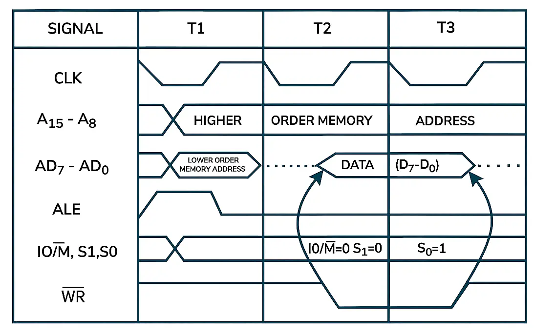
Figure 17.2: Timing Diagram of Memory write Cycle of 8085 Microprocessor