Input Output (I/O) Read Cycle of 8085 Microprocessor
The I/O Read Cycle of the 8085 microprocessor is the process by which the CPU reads data from an external input device or I/O port. Unlike memory read where data comes from RAM/ROM, in I/O read the microprocessor communicates with external devices such as a keyboard, ADC, sensor input, switches, etc. The instruction which initiates this machine cycle is typically IN port-address, meaning the processor will fetch a byte of data from a specific 8-bit I/O port and load it into the accumulator (A register).
The entire operation occurs in three T-states (T1, T2, T3) and involves address placement, control signal generation, data transfer, and final completion of read operation.
Steps involved in I/O Read Cycle
The 8085 I/O read cycle is explained step by step as follows:
- The CPU places the 8-bit I/O port address on the lower order bus AD0–AD7.
- The signal ALE = 1 goes high to latch this lower address externally.
- The control line IO/M’ = 1 indicates that this is not a memory operation but an I/O access.
- The CPU activates RD’ = 0 (active low) to request data from the I/O device.
- The I/O device places data on the data bus.
- The processor reads that data and stores it internally (finally into accumulator).
- RD returns to high (inactive) and cycle completes.
Signals Used
Different signals used by 8085 during the I/O read cycle are listed below:
| Signal | Description / Purpose | State During I/O Read Cycle |
|---|---|---|
| ALE (Address Latch Enable) | Latches 8-bit I/O port address from AD0–AD7 | High in T₁, Low in T₂–T₃ |
| IO/M’ | Selects I/O or Memory operation | High (1) → I/O operation |
| RD’ (Read Control Signal) | Enables I/O device to place data on bus | LOW (0) in T₂–T₃ (Active) |
| WR’ (Write Control Signal) | Used only in write cycles | High (1) → Inactive throughout |
| S0 & S1 Status Signals | Identify type of machine cycle | S1 = 0, S0 = 1 → I/O Read |
| READY | Adds wait states for slow I/O devices | High normally; Low = Wait State inserted |
| CLK | Drives timing of T-states | Continuous clock throughout cycle |
| A8–A15 | Higher address bus | Not used → Don’t care for I/O |
| AD0–AD7 (Multiplexed) | Carries address first, then input data | T₁ = Address, T₂–T₃ = Data from device |
Operation during each T-state
| Clock Period (T-state) | Operation Performed during I/O Read Operation | Signals Active | Bus Activity |
|---|---|---|---|
| T1 | 8-bit I/O port address placed on AD0–AD7 and latched | ALE = 1, IO/M’ = 1, RD = 1, WR = 1 | AD0–AD7 → Address, A8–A15 not used for I/O |
| T2 | Read request initiated to I/O device | IO/M’ = 1, RD = 0 (Active), WR = 1, ALE = 0 | AD0–AD7 switches to Data Bus → Device places data on bus |
| T3 | Data read by CPU and stored internally | RD = 0 → then 1, IO/M’ = 1, WR = 1 | AD0–AD7 → Data accepted by processor into Accumulator |
Timing diagram of I/O Read Cycle
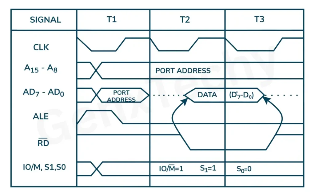
Figure 18.1: Timing Diagram of I/O Read Cycle of 8085 Microprocessor
Input Output (I/O) Write Cycle of 8085 Microprocessor
The I/O Write Cycle is the sequence during which the 8085 microprocessor sends (writes) data to an output device through an I/O port. Unlike the I/O Read cycle where data is taken in, this cycle transfers data out of the accumulator to a peripheral device such as LEDs, motors, display interface, DAC, etc. This machine cycle is initiated by the OUT port-address instruction. The process involves sending the port address first, then placing valid output data on the bus, and finally activating write control signals to complete the transfer.
Steps involved in I/O Read Cycle
The 8085 I/O write cycle is explained step by step as follows:
- The microprocessor places the I/O port address (8-bit) on the multiplexed bus AD0–AD7.
- ALE goes HIGH to latch and store this address externally.
- The signal IO/M’ = 1 indicates that this is not a memory access but I/O access.
- The CPU puts the output data (from accumulator) on the data bus.
- WR’ = 0 is made LOW to command device to accept data.
- The device latches/stores the data.
WR’ returns to HIGH indicating write completion.
Timing Cycle Details
To complete memory write operation 8085 microprocessor required three (03) T-states (clock periods) those are listed below in table:
| Clock Period (T-state) | Operation Performed during I/O Write Operation | Signals Active | Bus Activity |
|---|---|---|---|
| T1 | I/O port address placed on AD0–AD7 and latched externally | ALE = 1, IO/M’ = 1, WR = 1, RD = 1 | AD0–AD7 → Address output (later latched) |
| T2 | CPU places output data from Accumulator to data bus | IO/M’ = 1, WR = 0 (Active), RD = 1, ALE = 0 | AD0–AD7 → Output data to device |
| T3 | Data transferred to I/O port and write completed | WR = 0 → then 1, IO/M’ = 1 | Device reads data → AD0–AD7 tri-stated after transfer |
Control Signal Status
Status of 8085 microprocessor control signals during the I/O write cycle are listed below:
| Signal | Description / Purpose | State During I/O Write Cycle |
|---|---|---|
| ALE (Address Latch Enable) | Used to latch lower 8-bit port address (AD0–AD7) | High in T1, Low afterwards |
| IO/M’ | Selects operation type: I/O or Memory | High (1) → Indicates I/O operation |
| WR’ (Write Control Signal) | Tells I/O device to accept / write data | LOW (0) in T2–T3 (Active) |
| RD’ (Read Control Signal) | Used only in read cycles | High (1) → Inactive throughout |
| S0 & S1 Status Signals | Together indicate machine cycle type | S1 = 1, S0 = 0 (I/O Write) |
| READY | Synchronizes with slow devices | High normally; Low inserts WAIT states |
| CLK | Provides timing for T-states | Continuous clock pulses during cycle |
| A8–A15 | Higher-order address bus | Not used → Don’t care in I/O |
| AD0–AD7 (Multiplexed) | Carries address first, then data | T1 = Address, T2–T3 = Data |
Timing Diagram of I/O Write Cycle of 8085 Microprocessor
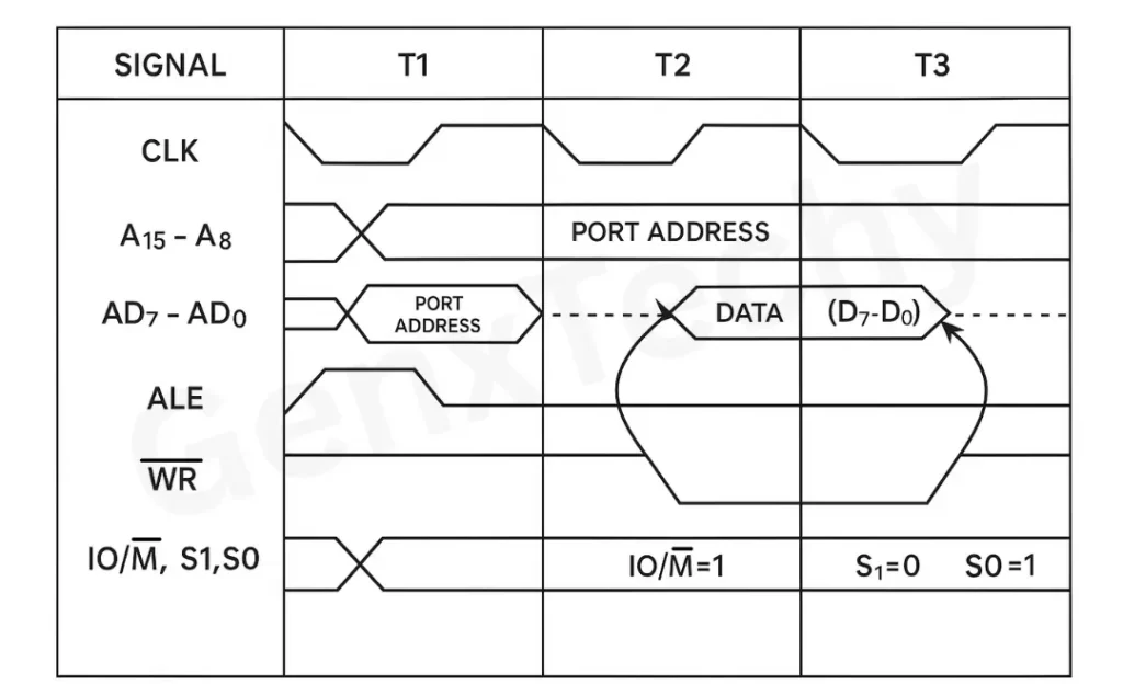
Figure 18.2: Timing Diagram of I/O write Cycle of 8085 Microprocessor