Design Methodology of VLSI Design
The Design Methodology of VLSI Design revolves around a structured and systematic process for creating complex integrated circuits (ICs). The process can be automated or semi-automated using Electronic Design Automation (EDA) tools to ensure accuracy, efficiency, and scalability.
Steps in VLSI Design Methodology
a) System Specification:
- The process begins with identifying a specific application or functionality.
- A system/device specification/concept is conceived and documented in a formal language.
b) RTL Design:
- The system idea is translated into Register Transfer Level (RTL) using Hardware Description Languages (HDLs) such as Verilog or VHDL.
- The RTL code describes the circuit’s behavior and structure.
c)Functional Verification:
- The RTL netlist undergoes compilation and simulation to ensure it meets the intended functionality.
- Iterative adjustments are made to refine the circuit behavior until the desired performance is achieved.
d) Constraint Specification:
- Constraints such as area, power consumption, and speed are defined.
- These constraints guide the synthesis and design optimization.
e) Synthesis:
- The behavioural description is converted into a structural description.
- This process generates an optimized hardware implementation that adheres to the constraints and produces the desired outputs.
f) Hierarchical and Abstraction Management:
- The design is broken into smaller, manageable modules.
- These modules are analyzed at different levels of abstraction to simplify the complexity.
g) Design Automation:
- Synthesis: Translating HDL into gate-level representations.
- Simulation: Verifying logic and timing.
- Layout: Generating physical designs.
- Testing and Verification: Ensuring functional correctness.
h) Hardware-Software Co-Design:
- Hardware and software components are designed concurrently.
- This reduces design cycle time and resolves compatibility issues early.
Design Styles in VLSI
1. Top-Down Approach:
- Starts with a high-level system specification.
- Progresses through successively lower levels of abstraction.
- Ensures that the overall system requirements drive the design process.
- Merits: Ensures system-wide consistency and easier integration.
- Demerits: Requires clear system specifications upfront.
2. Bottom-Up Approach:
- Starts with designing basic building blocks (e.g., gates, flip-flops).
- These blocks are assembled to create higher-level modules.
- Merits: Focuses on detailed design of individual components.
- Demerits: May lead to integration challenges at the system level.
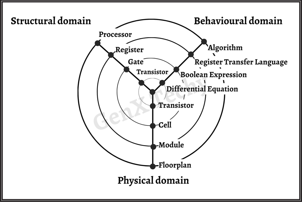
Design Domains—Y-Chart
The Y-Chart, also known as the Gajski-Kuhn Y-Chart, is a conceptual framework used in VLSI design to r0epresent the design domains and levels of abstraction systematically. It enables the designer to approach complex designs in an organized manner by breaking them into manageable parts.
Structure of the Y-Chart
The Y-Chart consists of three main axes as shown in Fig. 3.1, each representing a design domain:
a) Behavioural Domain: Defines the functionality of the system.
b) Structural Domain: Specifies the hierarchy and components (blocks) of the design.
c) Physical Domain: Focuses on the geometric and physical layout of the design.

Fig. 3.1 Gajski-Kuhn Y-Chart
Each domain is addressed at three levels of abstraction:
- System Level: High-level representation of the entire system.
- Register Transfer Level (RTL): Describes the flow of data and control between registers.
- Gate Level: Detailed representation of the logical gates and their interconnections.
