When we study the 8085 microprocessor, one of the first things to understand is how it uses its pins to carry information. The 8085 is designed in such a way that the lower 8 lines (pins) are used for two different purposes at different times. These lines are named AD0 to AD7.
- In one situation, these lines carry the lower 8 bits of the address (A0–A7).
- In another situation, the same lines carry the 8-bit data (D0–D7).
This sharing of pins is called multiplexing. It helps reduce the total number of pins on the chip, making the microprocessor more compact and economical. But the drawback is that the address and data cannot be sent at the same time on those lines. That’s why we need a process called demultiplexing.
Why Demultiplexing is Needed?
Let us try to understand the fact using a real-life example.
Imagine a classroom where the same board is used by two teachers. One teacher writes the class schedule, and another writes homework. If both try to write at the same time, students will get confused. The solution is to separate the information so that it is clear which part is the schedule and which part is homework.
- The same happens with the microprocessor. The lower address (A0–A7) and data (D0–D7) share the same bus lines. To avoid confusion, we must separate (demultiplex) them properly.
- The 8085 saves pin count by using the same set of lines for address (lower 8 bits) and data.
- To make sure the address is not lost when data comes in, we use Address Latch Enable (ALE) and a latch to separate them. Please refer Figure 1 to understand the concept of ALE.
- After demultiplexing, we get a proper 16-bit address bus and an 8-bit data bus.
How Demultiplexing Works
Demultiplexing means separating these two signals (address and data) so devices know when they’re receiving an address and when they’re getting data.
The 8085 uses a special signal called ALE (Address Latch Enable) to tells us when the lines AD0–AD7 are carrying the address and when they are carrying data.
- During the first part of the machine cycle, ALE goes high. This means the lines AD0–AD7 contain the lower 8-bit address.
ALE = 1 (HIGH): The AD0–AD7 pins carry the lower 8 bits of the address (A0–A7)
- An external latch (like the 74LS373 IC) is used to store this address. Once stored, it is available as a stable output A0–A7.
- After that, the same lines (AD0–AD7) are free to carry the data without losing the address information, since the address has already been latched.
ALE = 0 (LOW): The AD0–AD7 pins carry data (D0–D7).
i) During T1 clock cycle:
ALE goes HIGH → The latch grabs the address (A0–A7) from AD0–AD7.
ii) When ALE falls LOW:
The latch locks the address (keeps it stable).
iii) In later clock cycles (T2, T3):
AD0–AD7 is switched to carrying data (D0–D7), while the latch feeds the stored address (A0–A7) to memory/I/O devices.
Figure 1 shows the address and data demultiplexing using IC 74LS373
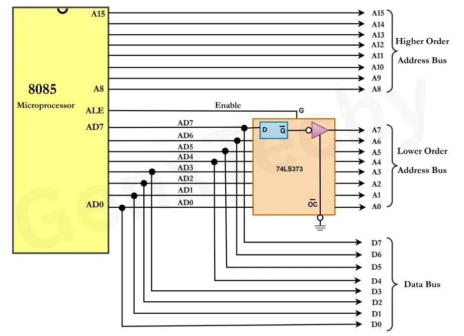
Fig. 1: Address and Data bus Demultiplexing