8085 Microprocessor Pin Diagram
Intel 8085 has 40 pins, operated at 3 MHz clock frequency, and requires +5V for power supply. The 8085 is available with 40 pins as a Dual in-Line Package (DIP). The signals can be classified into Seven (7) categories:
- Power Supply and Frequency Signals
- Data Bus and Address Bus
- Control and Status Signals
- Interrupt Signals
- Serial I/O Signals
- DMA Signals
- Reset Signals
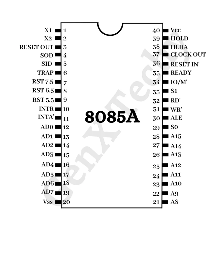
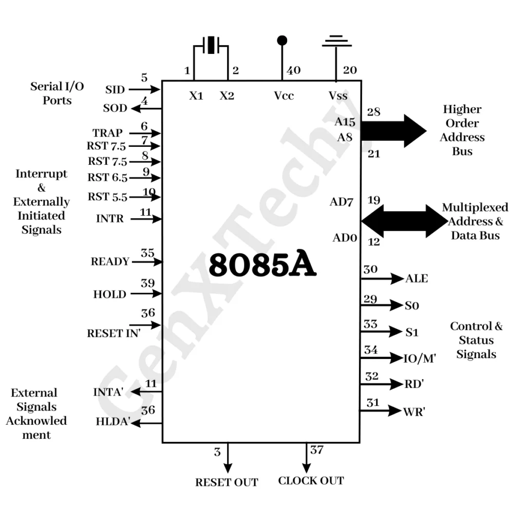
The pin layout and signal groups are shown in Fig. 1 and Fig. 2, respectively.


Fig 1 .8085 Pin Diagram
Fig 2. 8085 Signal Flow Pin Diagram
1. Power Supply and Frequency Signals
Following pins are available in the 8085 microprocessor to provide power and clock signal.
a) Vcc: Pin No. 40
It requires a single +5 V power supply.
b) Vss: Pin No. 20
Ground reference.
c) X1 and X2 (Input): Pin No. 1, 2
A microprocessor needs a square wave (clock) signal to ensure that all internal operations are synchronized. A crystal or R-C or L-C network is connected to these two pins. The crystal frequency is internally divided by two to provide the operating system frequency. There are three advantages in increasing the frequency of the crystal- as frequency increases, the crystal size becomes smaller, and the crystal becomes lighter and cheaper. Therefore, clock circuits include a divide-by-two circuit so that a double frequency crystal can be used. So, to run a microprocessor at 3 MHz, a 6 MHz crystal should be connected to the X1 and X2 pins. The crystal is preferred as a clock source because of its high stability, large Q (Quality Factor), and absence of frequency drifting with aging.
d) CLK OUT (Output): Pin No. 37
This signal is used as a system clock for other devices. Its frequency is half the oscillator frequency.
2. Data Bus and Address Bus
The 16-bit address bus and 8-bit data bus are spit into the following two groups:
a) AD0 to AD7 (Input/Output; Three state multiplexed address/data bus): Pin No. 12 to 19
The 8-bit data bus (D0 – D7) is multiplexed with the lower half (A0 – A7) of the 16-bit address bus. During the first clock period of the machine cycle (T1), lower 8 bits of memory address or I/O address appear on the bus. During remaining clock periods of the machine cycle (T2 and T3) these lines are used as a bi-directional data bus. The lines enter into the tri-stated high impedance state during hold and halt modes.
b) A8 to A15 (Output; Three-State Higher-Order Address Bus): Pin No. 21 to 28
The most significant 8-bits of memory addresses and the 8-bits of the I/O addresses are transported to these lines. Like the lower-order address/data bus, these lines also enter into the tri-stated high impedance state during hold and halt modes.
3. Control and Status Signals
The 8085 uses various control signals for fetching and executing instructions. The operations that take place upon execution are indicated by the status signals. Details of Control and Status signals are explained below:
a) ALE (Address Latch Enable) (Output): Pin No. 30
The AD0 to AD7 lines are multiplexed, making the lower address half (A0 – A7) accessible only during T1 of the machine cycle. However, this lower address portion is required for accessing specific memory or I/O port locations throughout T2 and T3. To maintain its availability, it’s necessary to latch the lower address during T1. This is accomplished using an external latch along with the ALE signal from the 8085 Pin Diagram.
b) RD’ (Output; Three-state): Pin No. 32
When RD is set to low, it indicates that data should be read from the designated memory location or I/O port using the data bus.
c) WR’ (Output; Three-state): Pin No. 31
Write is an active low signal that indicates that the data on the data bus is to be written into the selected memory or I/O location. Data is placed on the data bus at the trailing edge of the WR (bar) signal.
d) IO/M’ (Output; Three-state): Pin No. 34
IO/M’ indicates whether the read/write operation is being done with respect to the memory or I/O device. Logic 1 indicates I/O device access and logic 0 indicates memory access. The signal is tri-stated during hold and halt modes.
e) S0, S1 (Output): Pin No. 29, 33
These are the status signals used to specify the kind of operation being performed. The status signals combined with IO/M’ signals to govern various operations are listed below:
| IO/M’ | S1 | S0 | Operation (Data Bus Status) |
|---|---|---|---|
| 0 | 1 | 1 | Opcode Fetch |
| 0 | 1 | 0 | Memory Read |
| 0 | 0 | 1 | Memory Write |
| 1 | 1 | 0 | I/O Read |
| 1 | 0 | 1 | I/O Write |
| 1 | 1 | 1 | Interrupt acknowledge |
| 0 | 0 | 0 | Halt |
4. Interrupt Signals
These signals are used to make the microprocessor respond to high priority externally initiated signals. When an interrupt signal is detected by the process, it suspends the execution of the current program and executes the program corresponding to the interrupt signal instead. Various interrupt signals are explained below:
a) RST 7.5, RST 6.5, RST 5.5 -Restart Interrupt (Input): Pin No. 7, 8, 9
These three inputs are hardware interrupt signals. These are used to make the processor execute a subroutine at a predefined address. However, these interrupts do not have an acknowledgment signal.
b) TRAP (Input): Pin No. 6
Trap interrupt is a non-maskable restart interrupt. It is unaffected by any mask or interrupt enable signal. It is the highest priority interrupt.
c) INTR (Input): Pin No. 10
Interrupt request is a general-purpose interrupt. It is sampled only during the last clock cycle of the instruction. If INTR is high, the program counter (PC) will not be allowed to increment and an INTA (an active low signal) will be issued. Program execution can be shifted to the Interrupt Service Routine (ISR) by inserting an RST or CALL instruction on the data lines during this cycle.
d) INTA’ (Output): Pin No. 11
Interrupt acknowledge is an active low signal used instead of RD’, after an interrupt request has been accepted. This signal is used to read the opcode from the data bus and execute it.
5. Serial I/O Signals
There are two signals to implement serial transmission. They are serial input data (SID) and serial output data (SOD). The data bits are sent over a signal line, one bit at a time, in serial transmission.
a) SID (Input): Pin No. 5
This input signal is used to accept serial data bit by bit from the external device. The bit data on this line is loaded in the 7th bit of the accumulator whenever a RIM instruction is executed.
b) SOD (Output): Pin No. 4
This is an output signal which enables the transmission of serial data bit by bit to the external device. The output SOD is set or reset as specified by the SIM instruction.
6. DMA Signals
Direct Memory Access (DMA) is a feature that allows peripheral devices to communicate directly with the system’s memory without involving the central processing unit (CPU) for data transfers. This enables faster and more efficient data movement, as the CPU is freed from managing every data transfer. Following signals act as the DMA control signals for the microprocessor.
a) HOLD (Input): Pin No. 39
Hold is an active high signal used in the direct transfer of data between a peripheral device and memory location. Logic 1 on the Hold pin indicates that another controller, generally the DMA controller, is requesting the use of the address and data buses. The CPU, upon receiving the Hold request, will relinquish the use of the buses after completing the current instruction. An acknowledge signal is sent out by the processor and the address, data, RD’, WR’, and IO/M’ lines are tri-stated. The processor can regain control over the buses only after the Hold signal is removed.
b) HLDA’ (Output): Pin No. 38
Hold acknowledge is an active high signal, indicates that the CPU has received the Hold request and that it will relinquish the buses in the next clock cycle. HLDA goes low after the Hold request is removed. The CPU takes the buses half a clock cycle after HLDA goes low.
c) READY (Input): Pin No. 35
This signal is used to interface slow peripheral devices with the fast microprocessor. If Ready is high during a read or write cycle, it indicates that the memory or peripheral is ready to send or received data. If Ready is low, the CPU waits for it to go high before completing the read or write cycle.
7. Reset Signals
The reset signal of the 8085 microprocessor is a control signal that initiates a reset operation, restoring the microprocessor to its initial state. When this signal is activated, the microprocessor’s internal registers and flags are reset, and program execution begins from a predefined memory location called the reset vector address.
a) RESET IN’ (Input): Pin No. 36
This signal sets the program counter to zero (0000 H) and resets the interrupt enable and HLDA flip-flops. It is an essential signal for any microprocessor system because it determines the address at which program execution begins. In most microprocessor-based systems, RESET IN’ signal is applied as soon as the power is turned ON. A power-ON reset circuit is used to do this.
b) RESET OUT (Output): Pin No. 3
The output signal indicates that the CPU is being reset. It can be used as a reset signal for peripheral chips. This signal is synchronized to the processor clock.
