In the 8085 Microprocessor, the Opcode Fetch Cycle is the first and most essential part of the instruction execution process. It is the phase where the microprocessor fetches the operation code (opcode) of an instruction from memory to determine what operation needs to be performed. Every instruction execution in the 8085 begins with an Opcode Fetch Cycle.
Before understanding the Opcode Fetch Cycle, let’s understand what an opcode is.
An opcode (Operation Code) is the part of an instruction that tells the microprocessor what operation to perform.
Example:
- Instruction: MOV A, B
- Here, MOV is the opcode (it means “move data”).
- A, B are operands (data or registers involved).
So, every instruction begins with an opcode, which the microprocessor must fetch from memory before it can execute.
Opcode Fetch Cycle
Definition:
The Opcode Fetch Cycle is the process by which the 8085 microprocessor retrieves (fetches) the operation code (opcode) of an instruction from memory.
- The Opcode Fetch Cycle is the process of reading the opcode of an instruction stored in memory.
- The 8085 uses the Program Counter (PC) to point to the memory address of the instruction.
- The address is sent to memory through the address bus, and control signals are generated to perform a read operation.
- The fetched opcode is then stored in the Instruction Register (IR), where it is decoded.
Stepwise Operation of the Opcode Fetch Cycle
Step 1: The Program Counter (PC) provides the address of the memory location where the instruction is stored.
Step 2: The address is placed on the address bus and the ALE (Address Latch Enable) signal is made high to indicate a valid address.
Step 3: The control signals IO/M’= 0 (memory operation) and RD’ = 0 (read) are activated.
Step 4: The addressed memory location places the opcode on the data bus.
Step 5: The 8085 reads the opcode from the data bus and stores it in the Instruction Register (IR).
Step 6: The Program Counter (PC) is incremented by one to point to the next instruction byte.
Step 7: The opcode in the IR is decoded by the control unit to prepare for the next operation.
Step 1: Program Counter (PC) sends the Address
- The Program Counter (PC) holds the address of the next instruction to be executed.
- The address stored in the PC is placed on the Address Bus.
Example:
Let’s assume the next instruction is stored at memory address 2050H.
Status,
- PC = 2050H
- Address Bus ← 2050H
Step 2: Control Signals are generated
To read the instruction (opcode) from memory, the microprocessor sends:
- ALE (Address Latch Enable) = 1 (to indicate lower address byte on AD0–AD7 lines)
- IO/M’ = 0 (since this is a memory operation)
- RD’ = 0 (to read from memory)
- WR’ = 1 (not writing)
Step 3: Memory places the Opcode on Data Bus
- The memory uses the address (2050H) to find the stored data (which is the opcode) and places it on the data bus.
- Let’s assume that the opcode at 2050H is 3EH (which means the instruction MVI A, data).
Status:
- Data Bus ← 3EH
Step 4: Microprocessor Reads the Opcode
- The 8085 reads this opcode from the data bus and stores it temporarily in the Instruction Register (IR).
- Now, the processor knows which operation it needs to perform.
Step 5: Increment Program Counter
- After reading the opcode, the Program Counter automatically increments by 1 to point to the next memory address, where the next part of the instruction (like operand) may be stored.
Status:
- New PC = 2051H
Step 6: Decode the Opcode
- The Control Unit inside the microprocessor now decodes the fetched opcode (3EH) to understand what operation is to be done next.
- In this case, it recognizes that:
3EH = “MVI A, data”
which means Move Immediate Data to Accumulator.
Timing Diagram of Opcode Fetch Cycle
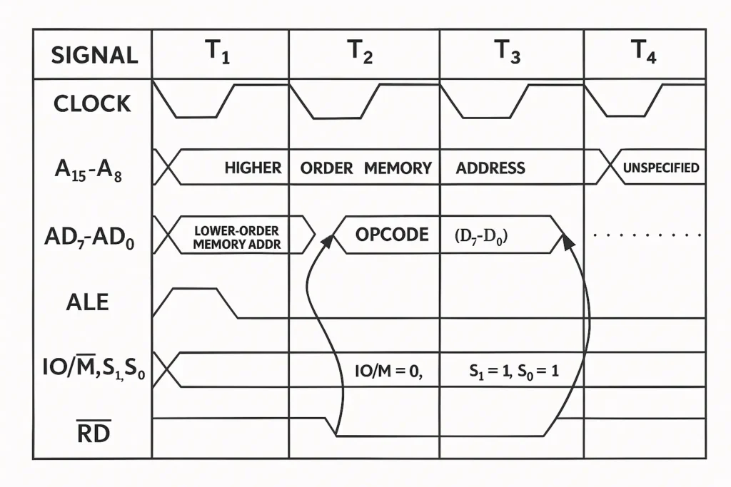
Figure: Opcode fetch cycle of 8085 microprocessor
Every operation inside the microprocessor happens in small time steps called T-states.
Each instruction takes one or more machine cycles, and each machine cycle consists of a few T-states.
The Opcode Fetch Cycle takes 4 to 6 T-states. Generally, actions take place in each T-state is listed below.
| T-state | Action |
|---|---|
| T1 | Address of the instruction is sent to memory (PC → Address Bus). |
| T2 | Control signals (RD’, IO/M’) are activated. Memory gets ready. |
| T3 | Opcode is placed on data bus by memory and read by CPU. |
| T4 | Opcode is decoded by microprocessor. |
Status of control signals during the Opcode fetch cycle is tabulated below:
| Signal | Description | Value during Opcode Fetch |
|---|---|---|
| IO/M’ | Memory or I/O | 0 (Memory) |
| S1 | Status signal | 1 |
| S0 | Status signal | 1 |
| RD’ | Read | 0 (Active) |
| WR’ | Write | 1 (Inactive) |
| ALE | Address latch enable | 1 (During T1) |
| INTĀ | Interrupt acknowledge | 1 (Inactive) |